


SRAM: the Silicon Dark Art
Logic tends to get all the publicity in chips, but most chips depend on a lot of SRAM.

Hidden in Plain Sight
When you look at a die photograph of a modern chip you will notice that much of the chip is made up of rectangular regions which generally look darker than the rest of the chip.

Mostly those will be the SRAM (Static Random-Access Memory) which is used as the working memory for the logic on the chip.
Some of the dark regions especially near the edges are analog designs. SRAM and analog appear darker because they do not use as many metals as the logic regions need, with more insulator at top which will reflect light differently.
My prior series about blockchain mining logic did not need any SRAM, which as I noted in the series is rather unusual, but I promised to get back to SRAM and here we are. I filled in a few holes in my own knowledge of SRAM and have found the subject very interesting. SRAM has always been a little different to the logic and the compromises necessary to fit both logic and SRAM on the same chip have caused continuing innovation in SRAM. The key features can be explained fairly simply and that is what I will try to do in the next few postings.
What is SRAM?
Static RAM has been used on logic chips since the earliest years of integrated logic. It is called “static” because it holds its value without needing refresh. The lack of refresh simplifies use, but the real value is that it is fast and can be made on the same chip as the logic. The other common form of working memory, DRAM, can be made about 10x denser than SRAM but it is much slower and also made in a quite different process than logic, so it ends up on separate chips. I may write about DRAM and Flash in future posts. This series of 4 posts will drill into SRAM.
Less is Moore
If you build one bit of memory in standard logic you get something like a D flip-flop.
The two NANDs to the left control access to the bit for writing, and the two NORs at the right are a pair of inverters in a feedback loop The feedback loop can be stopped when the enable signal is applied, allowing a data value to control which NOR is true and the other is false. When the enable signal goes to zero the inverters go back into the feedback loop holding the new value. It is a clever design used inside the logic for latches, but too big to be attractive for a large array of bits.
The classic SRAM circuit simplifies this to 6 transistors. It does this by some analog magic and brute force. Four of the transistors are used to make to inverters in a feedback loop, and one transistor on each side is added to allow data to access to the inverter loop.

The trick that makes this work is to size the transistors so that the feedback loop is relatively weak. The access transistors are made strong so that when they are enabled new data can be applied by greater current than the feedback loop, overpowering it with the new data. If you think that is tricky and liable to take a lot of energy if it's not done right then you are on the right track.
The word enable reaches all the cells in one word at the same time, generally either all cells in a row, or half the cells alternating even and odd on different enable wires. The DQ (data in and out) lines are the bits, in pairs carrying complementary values to match the complementary states of the inverter pair. In the drawings the words run left to right and the bits run top to bottom, when the SRAM is laid out in an array.
SRAM rarely uses the 6T cell because SRAM is closely combined with logic and usually needs to support parallel reads and writes which add more transistors and area. But the 6T cell is the best starting point to understand SRAM, then we can look at adding ports.
FinFET Needs Some Changes
Back in the days of planar transistors it was possible even with logic process to have different sizes of transistor. This was used to ensure the feedback loop was weaker than the access path. Planar processes had naturally weaker PMOS transistors than NMOS, due to hole mobility being less than electron mobility, so the PMOS transistor used in each inverter pair would give a weak drive. The NMOS transistors in the inverters were similar size, but the access transistors would also be NMOS transistors typically twice as large. This combination allowed the new data to overpower the feedback loop and force a new value in. If enabling of the access transistors was as brief as possible the amount of energy used for switching writing a new bit could be held below the femto-Joule level in planar processes. That was low enough.
When we switch to FinFET process, a difference in transistor strength has to be achieved by changing the number of fins. I will be using the Mock 4 rules explained in the Pipe 2 post but the memory cell uses a single fin per transistor.
Pipe.2: Imaginary Library of Useful Logic Cells

In last week’s post we established some of the context. I am building an imaginary cell library inspired by a 4-nm FinFET process, because I want to estimate the size and performance limits of a BlockChain hash ASIC. And to really understand how it all works, layer by layer.
One of the advantages of FinFET is the use of stressed channels so the PFET is about the same strength as the NFET. As a result, in the 6T SRAM the P driver is no longer weaker than the N driver unless the fin count is changed. Even if you could change the number of fins the classic ratio of 1:2:4 drive strength for inverter P, inverter N, and access channel strengths would be difficult to manufacture in recent process nodes. When it came to FinFET a lot of rethinking had to be done on how to build an SRAM cell. The main focus was on avoiding the need for size-based strength ratios. The techniques that were invented are generally described as assists. Two main kinds of assists are used. One is to increase the strength of the access transistors by using a boosted gate voltage to turn them on more strongly than the other transistors. The other method is to reduce the cell voltage, the Vdd, to make the cell weaker relative to the voltages of the new data values. We will use the boosted gate as it seems most common and is simple to integrate with the enable driver and timing. Boosting the cell Vdd has potential complexity since power and ground have their own rules for layout, avoiding droop, and capacitive reserve which all need to be solved.
The Classic FinFET SRAM Layout
Let’s put the assists aside and first look at what happens to layout when FinFET rules are used. The transistors will have equal geometries, and generally follow the same guidelines as the logic process, but SRAM cells use transistors with just one fin, even when the logic transistors may use 2 or 3 fins. This means the track heights will be different than the logic cells but the lithography process can be the same if we simply do not apply the final etch doubling to the SRAM fin preparation.

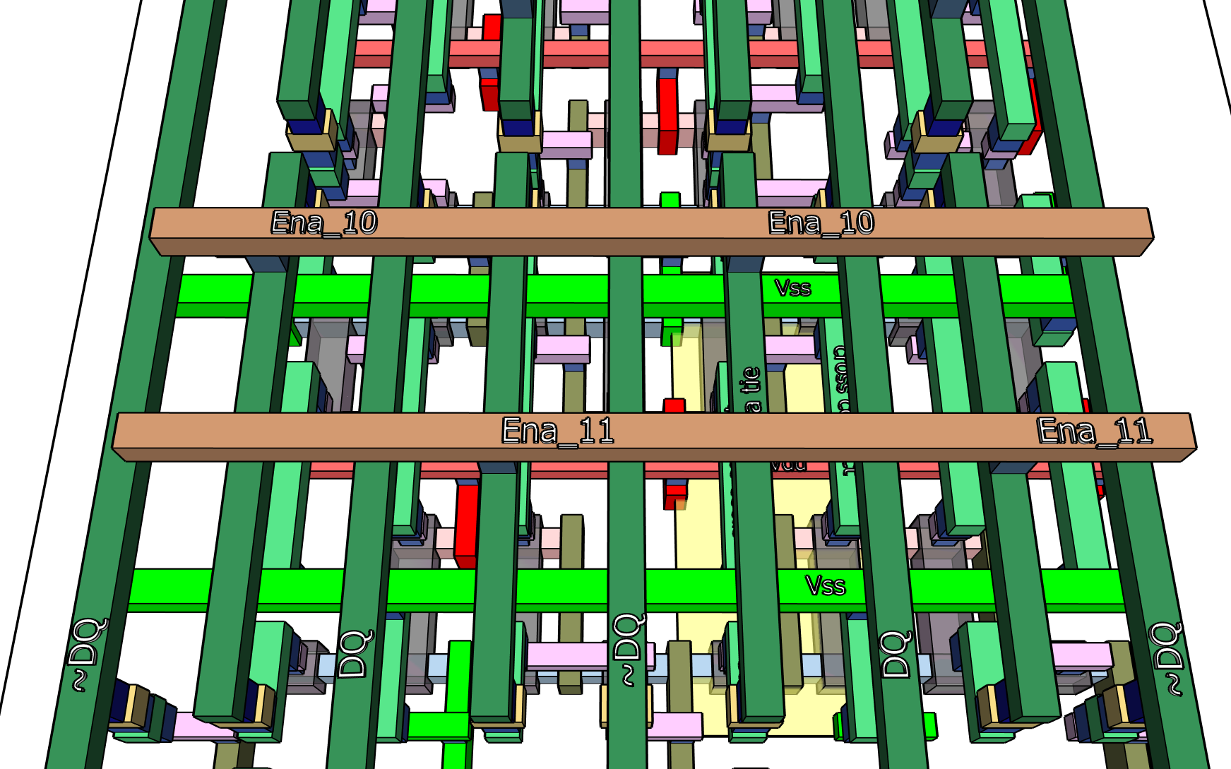
On the left we take the 6T form drawn in ordinary style. The 4 transistors in the middle are the inverters connected for feedback, while the two outside transistors are access channels which are gate-enabled where the data value may be written or read. The conventional name DQ is given to these lines which may act as Data-input or Data-output. This is a single “port” for access to the memory, the most basic of SRAM functions.
The most common 6T SRAM layout is shown in cartoon form above. This form has shared elements on all four sides which saves on area (side to side) or simplifies the chip process (vertical alternation of P and N fins in pairs). There is almost no empty space when the neighbor cells are reflected layouts at each boundary:

That layout is crazy fun. The reflections have some side effects. Obviously the peripheral circuits are going to need some reflected elements. More importantly, sharing the data lines (the DQs which move data values both in and out) means that a cell cannot be activated at the same time as its neighbors. What looks like one row will actually behave as two logical rows each half the elements (odd or even columns) and there will also be some disturbance effect on the idle cells between the active cells when a row is in use.
Let’s build up that single cell, and some neighbors, using the same Mock 4 rules as we used for the SHA-256 logic. We can start with the fins, gates, and source/collector.

You may notice the 4 NMOS transistors at bottom and top, and 2 PMOS transistors in the middle. The metal-0 is added next

but, except for the Vdd rail, metal-0 does not connect to anything yet. This design was crowded and metal-1 is more interesting:
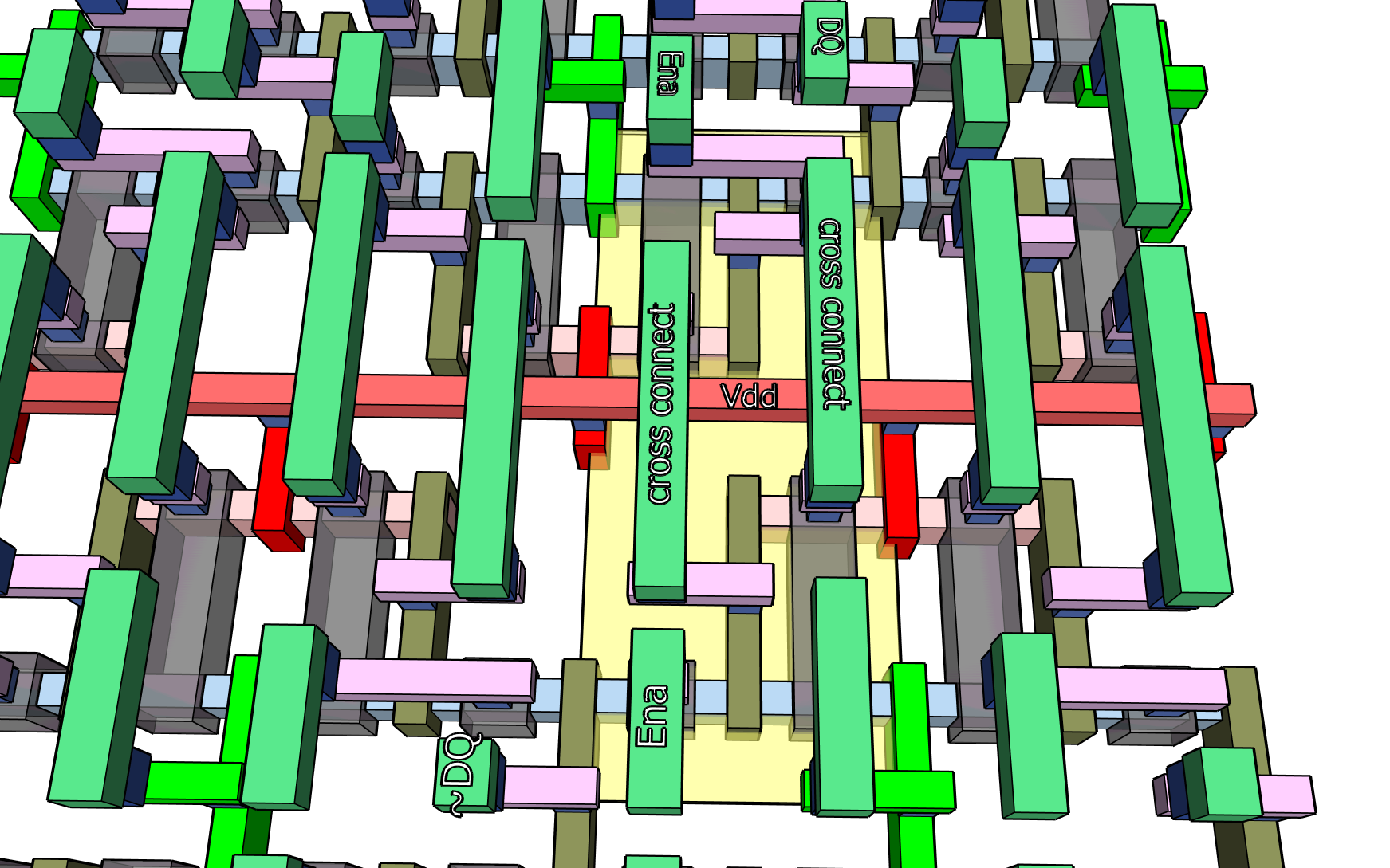
Now we can see how the inverters cross-connect to make the static bit in the center. We can see the DQ connections will be at bottom left and top right, while the word enable connections are going to arrive at top left and bottom right. Take a moment to compare this to the schematic drawing above, before more metal starts to hide it.
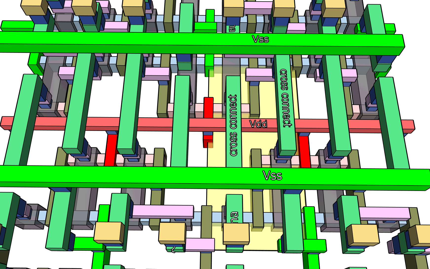
The metal-2 layer is mostly empty due to crowding on metal-1 pushing us up to metal-3 to get more connections between the top and bottom parts of the cell. If you look at the M1 in the image above you will see it is completely full, acting as a barrier to more connections at that level.

Next, finish the connections at the M3 level which becomes, in turn, instantly full. Fortunately, the remaining functionality is the word selects, which
are easily provided and connect to M3. Here is that sequence again in a video:
Not Happy with That
Not at all. It is nicely compact - in Mock 4 rules a size of 24,000 nm^2 is indicated - and should coexist with logic on the same device. But it was just the basic functionality, and it was 100% crowded on several levels. The Vdd line in metal 0 has no connection to upper metals, which is too thin a wire for a long run. This feels overly complex and is not a good starting point for adding ports.
Next Week
This forms a good starting point for understanding SRAM. Next week we will look at breaking the rules, a carefully modified Mock 4, that will greatly simplify the layout, and then we will add a second port to see how much the size goes up when we change to the kind of functionality needed for a more useful SRAM that works better with modern logic. In particular we will look at adding ports for simultaneous access.
After that we will return to discussing the assists and some of the peripheral logic, and in the 4th week we will design a small SRAM array and estimate a formula for how much overhead is needed in the periphery as the size of array scales. Spoiler: real-world SRAM size per bit is much more than just the size of the cells.
The approximately equal strength of PMOS and NMOS devices seen on newer processes is a result of strained silicon, which was introduced on planar processes. The amount of strain in the first generation of strained silicon wasn't sufficient to achieve equal mobility but it did reduce the mobility gap between PMOS and NMOS devices. With increasing strain in newer process iterations, after 3 or 4 generations PMOS mobility exceeded NMOS, delivering the results that you noted. This aligned in time with the FINFET transition. This differential impact occurs because it is easier to deliver large amounts of compression (benefiting hole mobility) to PMOS devices than to deliver similar amounts of tension (benefiting electron mobility) to NMOS devices.
Hello, what application did you use to generate those layouts and view them in 3d?