

In last week’s post we established some of the context. I am building an imaginary cell library inspired by a 4-nm FinFET process, because I want to estimate the size and performance limits of a BlockChain hash ASIC. And to really understand how it all works, layer by layer.
We could design every chip down to the transistor level, but that is impractical for anything large. Instead, the low-level design is done in advance to prepare a library of standard logic and functional cells which experience has shown are enough to make good designs of larger sets of logic. In commercial libraries there may be hundreds of cells that have been designed in detail, but by the time you have 30 of the most-used cells the advantage of the remaining cells is marginal, compared to simply making those cells by using some combination of the more common ones. Also, some of the clever circuits may have drawbacks like reduced output drive which limit their use.
For our purposes here we will just explore some of the most useful.

The process nodes have been pushed to the limits of lithography causing constraints on the design which require regular and repetitive layout. This allows patterns in optical projection to be exactly placed with uniform interference patterns and reduces error rates. The effect on circuit design is to rule out arbitrary placements at the smallest levels. The cell designs here are quite conservative, avoiding awkward placements. EUV may allow some arbitrary placements, but even with EUV as we go to smaller nodes the stricter rules may come back, so avoiding the those placements may give better insight for how future leading edge nodes work.
In one respect the SHA-256 project is very unusual. It does not use SRAM. There will be some use of latches to sample and hold values at clock edges between pipeline stages, but latches are not built the same way as SRAM. In most projects the SRAM is quite important, indeed if you look at die shots (images) of custom chips like
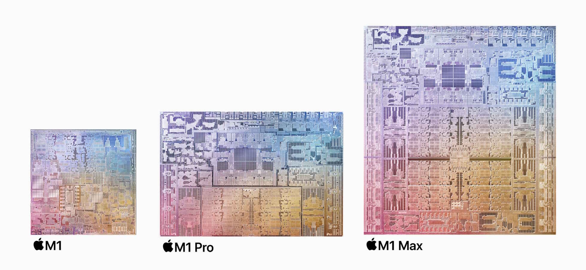
Apple M1 dies : billions and billions of cells, mostly SRAM.
the majority of a typical chip is SRAM, not logic. SRAM is therefore highly optimized and uses different design rules than the logic blocks. I will have a later blog post to discuss SRAM since it is important, but I will not give it as much attention as logic. Another post will go over the basics of DRAM, which is even more distant from logic process, so that readers will have an understanding of the forms of memory and the compromises that occur when trying to use them together with logic.
The Cells Chosen for the Library
The cells chosen for the logic library are:
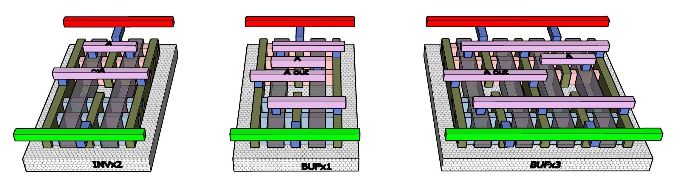
Inverters and buffers. Inverters do have a logical function (NOT) but they are also the most basic amplifier available. Put two inverters in sequence and they become a positive repeater that can boost signal - a buffer. Inverters are often found embedded inside more complex cells since negation is often useful to optimize the internal form of a function.
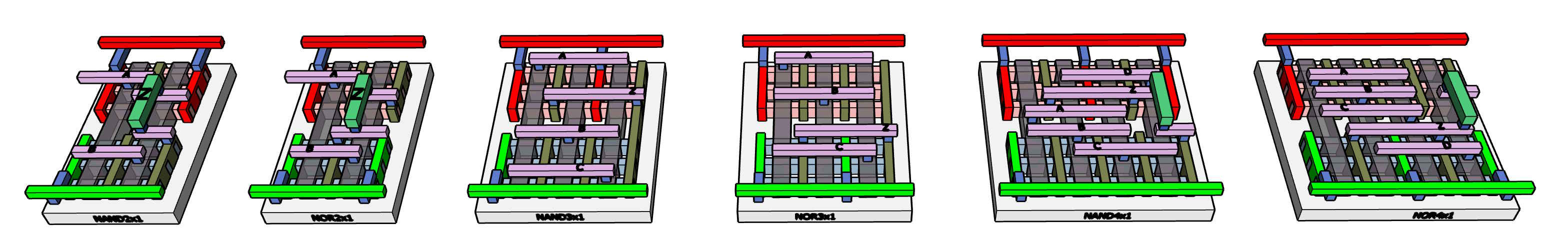
NAND and NOR. These are very common functions. There are some forms of logic analysis which use them as universal building blocks both because logically they are primitives that can make anything, and because physically they have transistor combinations which are simple and fast. The library will include 2-, 3-, and 4-input versions of NAND and NOR. These are closely related designs which are mirror images in terms of transistor layout.
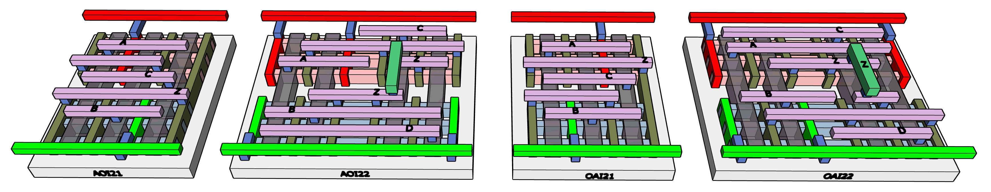
A set of cells with medium complexity and useful optimizations. The most commonly used are “or-and-invert” and “and-or-invert”, commonly abbreviated OAI and AOI. These sequential logic patters can be used to build several other common functions, such as XOR and ADD. They are useful because they have quite effective optimized transistor layouts, a little surprising since AND and OR are not themselves efficient layouts (you may notice they have not been in the list). There are multiple versions of these with different numbers of inputs: we will show implementations for OAI21, OAI22, AOI21, and AOI22.
A couple of other useful medium cells are XOR2 and AND4. The XOR cell can be built with AOI building blocks but this function is very widely useful and there are some improvements in layout which are possible by merged layout, which do not happen when separate library cells are used. AND4 also has a nice layout based on NOR4 and is important to one kind of fast carry look-ahead.

Next are a couple of medium cells which are especially useful for SHA-256, the MAJ3 (true if at least 2 out of 3 inputs are true) and MUX21 (third input chooses between first and second inputs to pass through). These each have significant optimizations over just combining simpler cells.

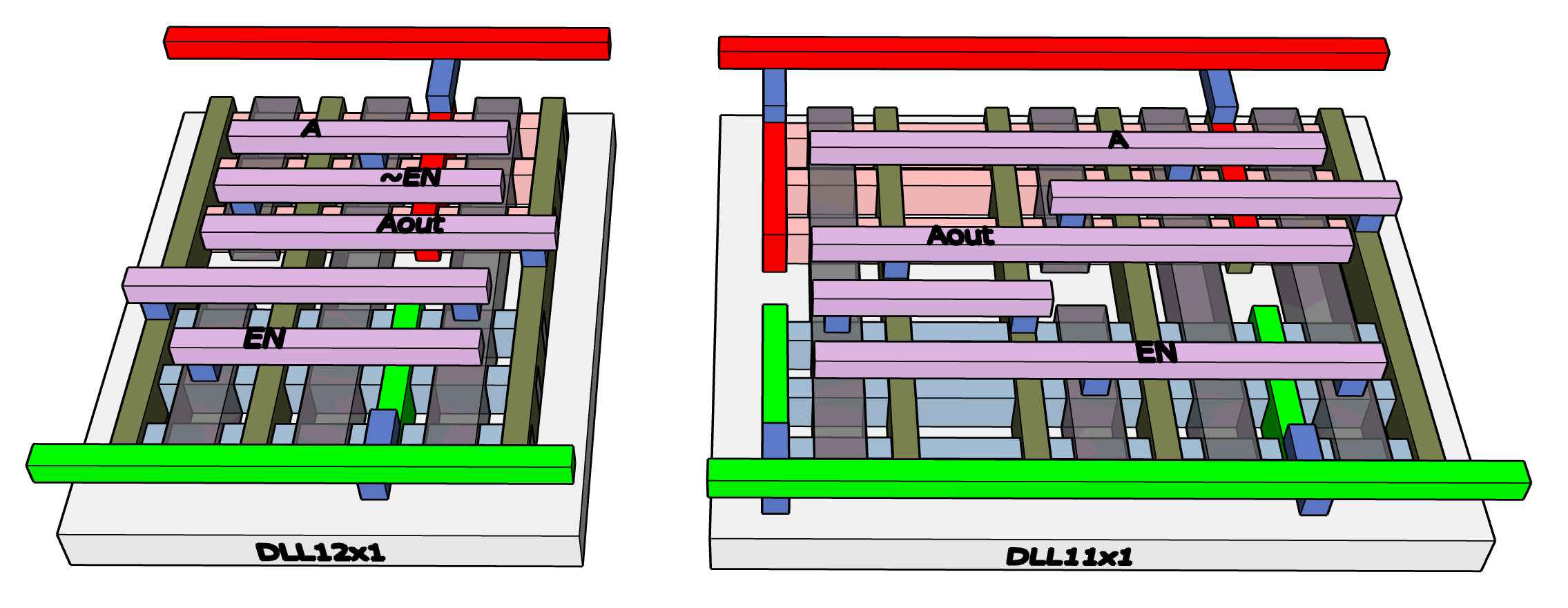
Dynamic latches with varied output strength (DLLx1, DLLx3). The blockchain miner never pauses (and if it does, its state will be discarded and it is restarted) so there is the unusual opportunity to implement the storage aspect of clocked logic storing charge on the gate capacitance inside the cell. This trick does not work reliably if the clock rate falls below about 50 MHz, but the miner will likely be running at 500MHz or even much faster. The dynamic latches fit in a smaller area and use less power than flip-flop latches, and you may remember I was mostly interested in using the least energy per hash operation so saving energy on clocking is valuable.
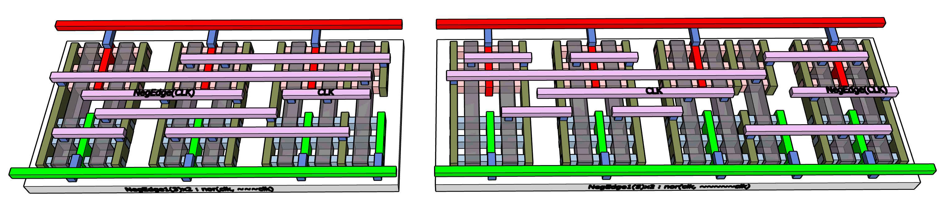
NegEdge(CLK) generators. These convert the 1-to-0 edge of the clock into a short pulse which can be used to drive dynamic latches or flip-flops. There are other circuits needed for clock distribution, which are out of scope here. The blockchain mining chip has a rather unusual clock distribution pattern which means that the clock circuits I want to use are not going to be that much help for other projects needing more conventional clocking. This will be discussed further when we put SHA-256 together.
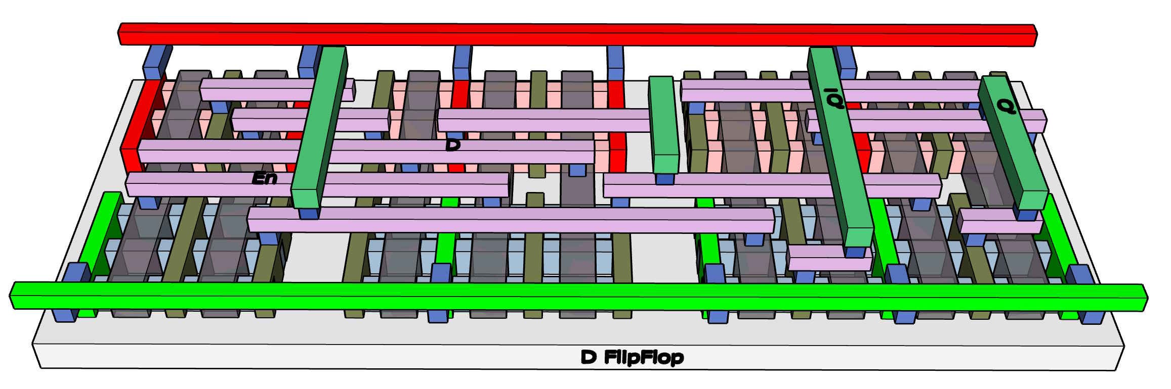
A D Flip-Flop. We may be using some flip-flops at the start and end of the pipeline, and it is nice to have them as a more conventional clocked latch to compare to the DLLs.
Full Adders. These are the largest cells in my library, and by far the most complex to lay out. I have three versions. One is, like all the smaller cells, laid out as a single track. That means all the logic flows between transistors left and right, not above or below. The track is bounded by the Vdd (positive) and Vss (zero, ground) power rails.
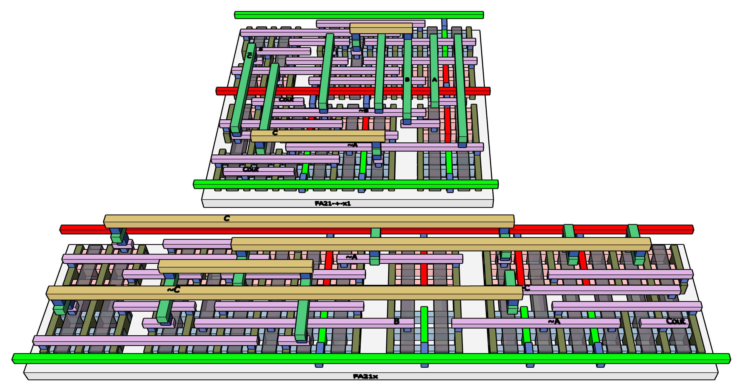
The single track results in crowded wiring. Dual-track versions allow for much less crowding as connections can be made in 2 directions.
This is more than 20 distinct functions. In practice each of these can be generated in 4 different forms: unchanged, reflected horizontal, reflected vertical, and rotated 180. The horizontal reflection allows optimizations for signals flowing left to right vs. right to left, while the vertical reflection is needed since tracks alternate with Vss-Vdd or Vdd-Vss order from bottom to top. EDA layout tools generally handle this automatically.
Some Things are Missing
The library uses a static logic approach, so there are no library cells for dynamic, domino, or other clocked logic. All of those add gates which add capacitance, and their benefits for low power design are mostly around controlling leakage and switching idle logic completely off. The HashPipe logic is always running, with around 50% logic change on every cycle, so none of that is really a saving in this design. Indeed, the dynamic switching will move the change rate closer to 100% as well as adding capacitance. So, this library is entirely “classic” static cells, except for the dynamic latches used to sample and hold values between pipeline stages.
SRAM is missing. Some conventional clock distribution logic is missing. Some kinds of useful flip-flops are missing. There are no half-adders, since I only need a small number and they are efficiently built from other cells. Some other drive strengths for various cell types might be desirable. Wider multiplexers will be found in commercial libraries, as well as cells for shift and rotate, and multipliers and dividers.
This project is not a full library. I am working through enough cells for my purposes, as well as a few I do not need but which show good examples of how to extend the library in ways I saw as useful to show basic principles. The rest is left as an exercise for the readers! Feel free to leave comments about any cells you are inspired to create.
Wiring Complexity
The wire crowding in this cell library is not severe. Only the full-adder cells use more than 2 levels of metal, and more than half the cells can be laid out with just M0 for internal connections. All inputs and outputs remain easily accessible. A real process may have 10 or more layers available for signals. Those layers make automated routing practical.
A shorter stack of layers is easier for a human to visualize and use in a manual design. The SHA-256 pipeline should be feasible with much less than 10 layers. I expect the pipeline to take advantage of abutting (adjacent) cells for most connections, sometimes using layers as low as metal 1 or 2. Thus, I value the reduced wire crowding more than folks who use automated tools and have designs where abutting is not so important. The HashPipe is fun to design manually, but real chips have larger problems of layout and routing.
Next Post
In the next post I will go through the basics of cell library in order, showing the logical circuits and explaining how these transferred into 3D cells.