Pipe.4: The Larger Cells
Useful Optimized Composite Functions
Last week we covered the general principles of constructing the chip and how the gates, vias, and wiring are layered on top. Then the basic gates of the library were introduced. This week we progress to some larger functions which can be optimized better than simply wiring up the primitives. In general “better” means smaller, use less energy per operation, and faster, though sometimes just 2 out of 3 improve.
OAI and AOI
The Or-And-Invert and And-Or-Invert functions are common patterns in logic which happen to have very compact expressions in transistor logic. There are different input counts for this, our cell library has the smallest ones, with 2 inputs to the first function and a third input to the second function:
Our basic set also includes the next wider pair, with both a third and a fourth input to another first-stage function.
AOI and OAI are another pair which mirror each other if the power rails swap.
These and other cells have weak output drives, so if they must fan out then there needs to be some buffering.
AND4 and OR4
These are mildly optimized from NAND4 and NOR4, which are included in the video so you can see what is happening.
The NAND4 and NOR4 have an available edge with power where it is easy to join an inverter to reverse the negation and reveal AND and NOR, as well as improve the output drive.
This inversion can be added cheaply where a function has an unused powered edge. The powered source/collector is enough isolation that we do not need a diffusion gap to keep the function blocks from interfering with each other. Sometimes single inversions can be used instead of full buffers, by splitting one buffer into two invertors in an equivalent logic. The EDA tools may understand this kind of transform so that cells like this do not need to be in the library, but we include them here for convenience in the manual layout.
More cell designs continue below the divider for paid subscriptions. Each week will have part of the blog open to all, then details then below a divider. The open part will help you judge if the work is of value to you, and I will try to keep it interesting by itself.
Thank you for supporting this work!
Opposite and Equal
The XOR and XNOR (equality) functions are surprisingly complex circuits for what are commonly perceived as simple logic. The OAI and AOI form part of the optimal simplifications for these:
Yet again, we have a power-mirrored pair of functions.
We could also use the powered edge to make a NOT so that XOR is NOT-XNOR if we want to make a version with a stronger output to drive more loads.
XOR3 will be used in a Full-Adder. That version is specialized to work inside the adder where both normal and inverted versions of the 3 inputs are available.
Majority and Minority of 3
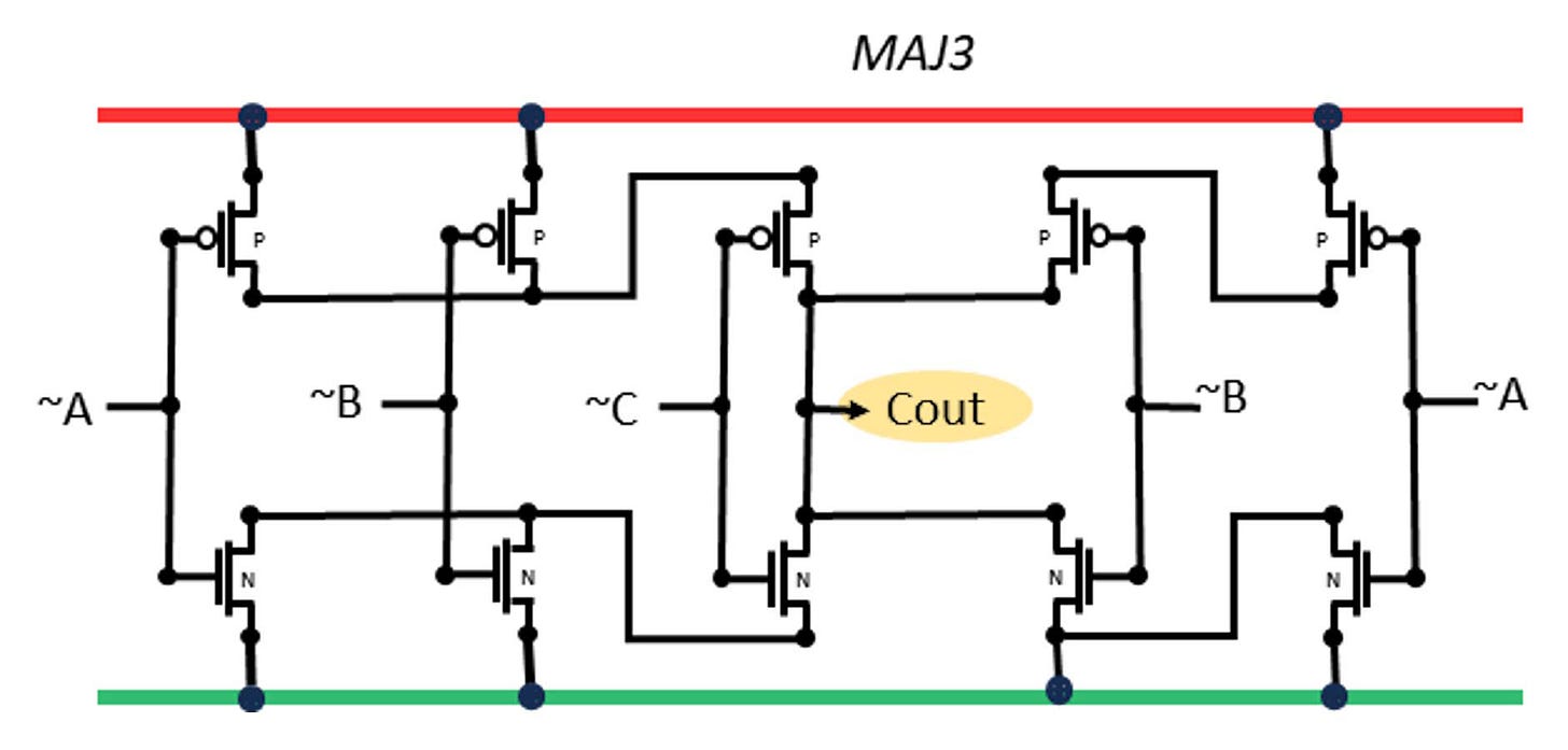
The majority-of-3 function here is built as the available-edge negation of a minority-of-3 circuit. There is also a MAJ3 implementation which inverts all 3 inputs, a situation which is sometimes easier because those inversions may be available because they are shared with other logic, as is the common case in some full adders.
The Majority function is identical if mirrored with a power rail swap. The Minority function is obtained by using non-inverted inputs.
That means we can also build a Majority as NOT-Minority(A,B,C), using the exposed power edge for a cheap inverter. That is the circuit shown in the video:
It can be useful to have that extra drive from the NOT (INVx1) output and is better like this if the inverted inputs are not available. The SHA-256 function has some need for this, while the inverted-inputs version can be found later in the full-adder.
MUX211
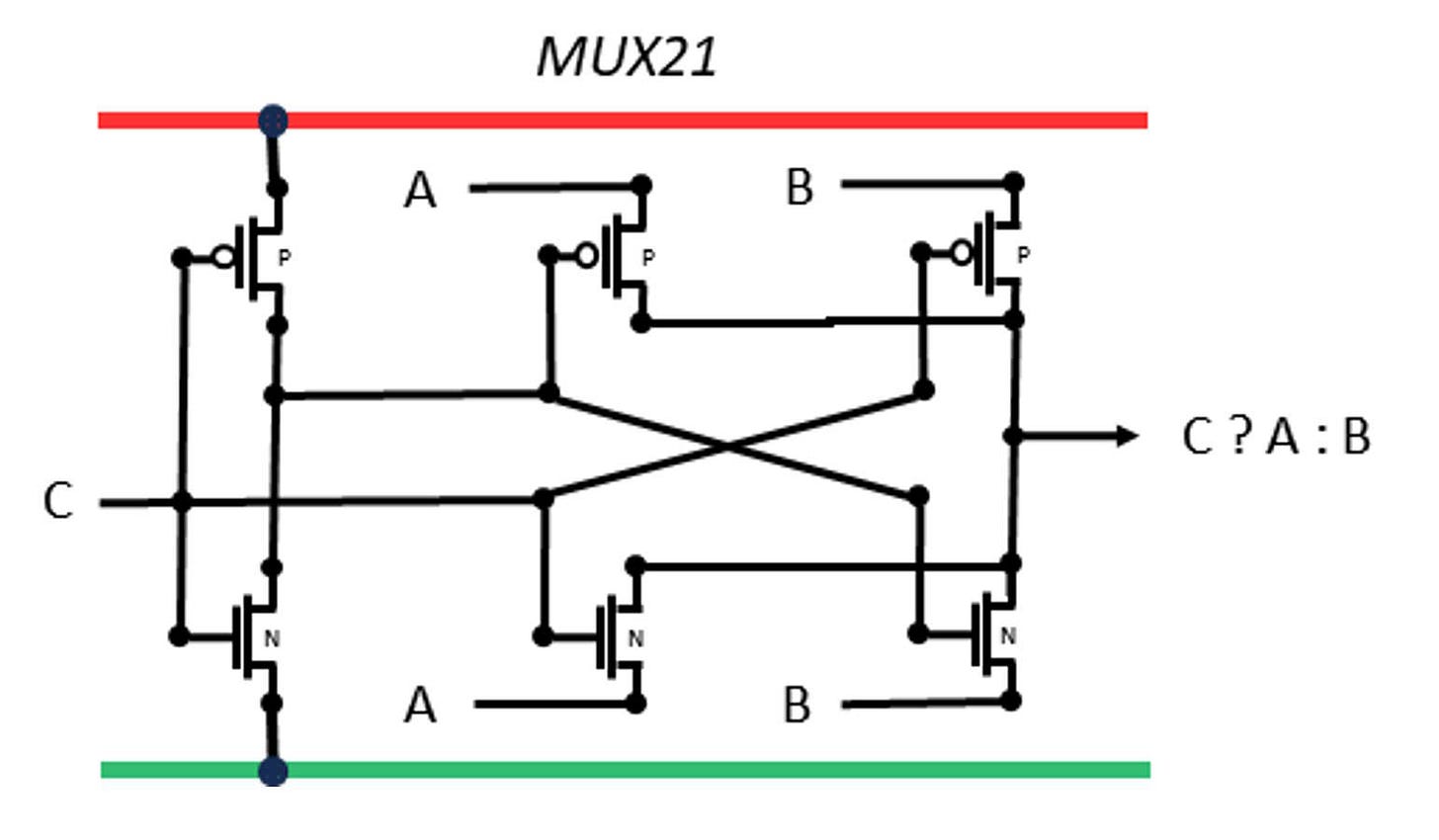
A multiplexor chooses inputs according to the third input. In this case Z = C ? A : B
This is a rare situation where the gate is split between P and N sections. The effect is to create a passing-gate. The selection signal C is inverted and then C:~C or ~C:C allow either A or B to pass.
Two versions are provided, the smaller version has weak drive and slightly higher input loads. The larger version has inversion on inputs and outputs to reduce the input load, improve timing, and strengthen the output drive.
Dynamic Latches
Latches are memory cells, but instead of being part of an array where a row of memory cells may be selected by an addressing mechanism, latches are individual memories generally directly connected at their inputs and outputs. A major use of latches is to sample a value when it has reached its stable state, and then hold that value for output while allowing a new input to be calculated without disturbing the output. Thus, a latch is also enabled to read its input, then disabled to hold the input.


Dynamic latches are like (dynamic) DRAM, they hold the value in charge on a capacitor. That charge leaks away so eventually the cell needs to be refreshed. In the case of a latch that means there is a limit to the time until the next enable. The capacitance is provided by the output gates of the latch, which are about 100x smaller than the capacitors in a DRAM, and in addition the low voltage transistor in low voltage logic will leak more than a DRAM access gate. A rough calculation suggests the hold time for 10% charge loss is around 100ns, about a million times shorter than a DRAM hold. However, the BlockChain clock rate is expected to be at least 500 MHz, so we only need a hold time of 2ns.
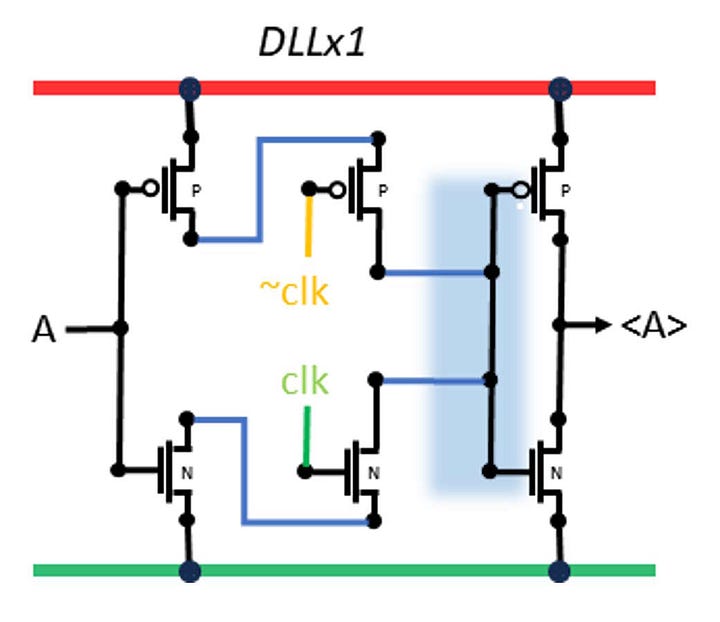
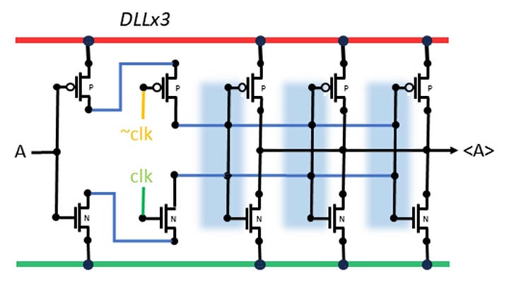
Two sizes of dynamic latch are shown, with 1 output pair, and with 3 output pairs. The 3-output version can drive more load but it also has 3x the capacitance to hold the value, so it will operate at lower frequencies if needed. The blue shading indicates where the charge is being stored, on the gates of the output transistors. The input is enabled by pulsing a clock and its negation to enable pass-transistors. The inputs are negated since the outputs are negated, so the overall effect is a buffer, and also to ensure a strong current flow during the brief enabling pulse.
What is the reason for using this unstable circuit? It is smaller and consumes less power than the D FlipFlop, the more conventional alternative. The SHA-256 pipeline uses a lot of latches, so this savings will be significant.
A D-FlipFlop
A D FlipFlop is the ordinary form of latch, in static logic that will hold a value however long it is until the next enable. This is the largest cell yet, but it is composed of some simple parts we have already seen:
The heart of a FlipFlop is a pair of NORs, used as inverters connected circularly to create feedback. Each NOR has an input which is zero when the DFF is not enabled, so they operate as feedback. However, when enabled the D input will block one of the NORs and force the other NOR to be inverted, setting the new value. As enable is released the feedback loop resumes to hold the new value.
This circuit runs out of space on M0 and needs several M1 bridges to complete the circuits. The use of M1 does not interfere with signals passing parallel to the fins, which is what you might think from first glance. The M0 pass underneath just fine, and the next level M2 will also not be blocked as they pass overhead. The only concern is the reduction of M1 available for other purposes. The blockage here is not enough to be serious.
Bridging adds resistance to the signal path mostly from the vias, which despite being small typically add as much resistance as a micron of wire. The use of a single layer of bridging is not a serious adder inside the circuit due to short wires and single loads on these paths. On the Q output it could be more important, but the Q output is weak already and likely to feed a buffer, so Q will most likely drive just a single load and the additional resistance will be a minor fraction of latency on the output.
Next week
In the next post we will look at clock pulse generation and then explore how to build adders - half adders, full adders, and carry look-ahead.


Fascinating.
Thank you for that. Having been involved in a couple of tape-outs todate, I wanted to see a clear picture of this side of the stuff my team was putting together. Understanding entails - and usually follows - identification. This really helps.