


Pipe.1: A Pipe Dream
A Thought Experiment in Silicon

For a few years I have been tinkering with projects which will need their own silicon chip. One in particular is a BitCoin BlockChain mining chip (the “HashPipe”). There are chips on the market already, but I was curious to understand the limits to efficiency of mining, and the size of the problem seemed just right. Not so small as to be trivial, not too large for one person to do. It was also a good place to start because it was not as important to me as some other projects, and those other projects would benefit from me learning from the HashPipe design.
The project was not as straightforward as I thought with some twists and turns and some resets, but eventually I started to see good progress. I built up an understanding which might be interesting as the basis for a set of blogs to explain what I had learned for others who may be interested in the subject of silicon design, so here we go.
Getting Started with Logic Design
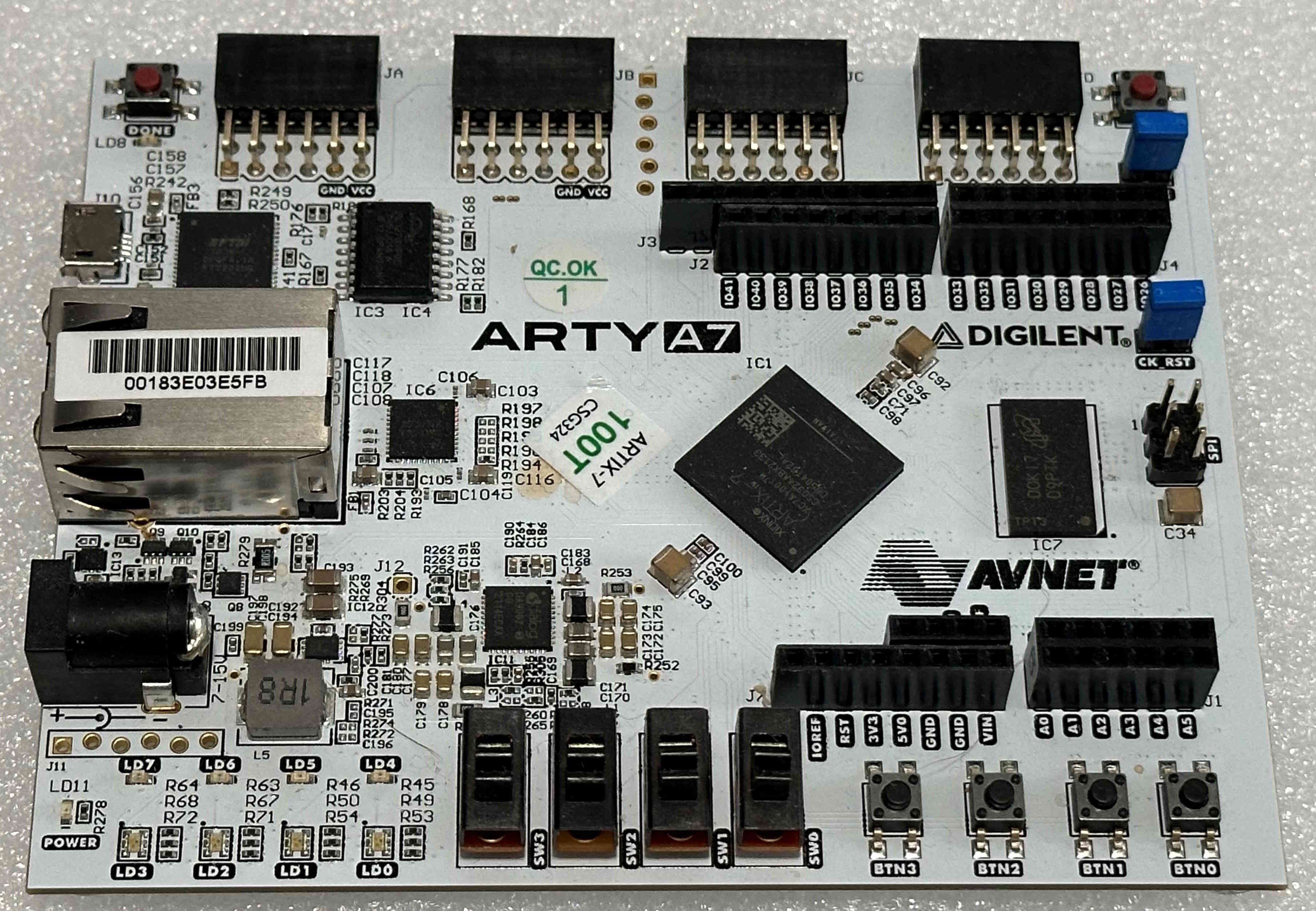
I started by using FPGA ‘s to ramp up on Verilog and ensure my design ideas worked. I used the Xilinx Artix 7 series and I was able to find plenty of application notes and good blog pieces showing how to use the tools and get started with a USB-connected board. My background is in software, I’ve always worked at the boundary between the hardware and software but the last time I worked on the hardware side a wafer was 4 inches in diameter. The free Xilinx Vivado tool is suitable for creating Verilog and operating a nice inexpensive board like the Arty A7. It feels a bit like using an integrated software development environment from the 1990s targeting a serially connected microprocessor. I did find that Vivado works a little better on Linux than it does on Windows. Not a big deal though. You should use Vivado on whichever platform you’re familiar with first while you’re learning it, and the online tutorials are applicable to both.
It is often said that software people can’t understand hardware because of the parallelism, but that doesn’t really seem true. There are a few quirks you need to learn about Verilog, such as the timing implications of the alternative forms of assignment but those reflect Verilog language choices rather real problems with parallelism. After a while you get used to it just like any other programming language. To be sure, you do need to think about operations in parallel, and you need to think about timing. That is, after all, part of the essential charm of using hardware. But if you’ve come to hardware with a particular project in mind you probably already have some idea of what you want to do there. You’ll get better at it with practice but there is no intellectual barrier for a programmer to become adept at hardware. The same sort of attention to detail and algorithmic thinking applies in both domains.
The next thing I wanted to do was to license an EDA tool like Synopsys, Cadence, or Siemens which will support ASIC design, not just FPGA. This proved to be something of a brick wall. Trying to reach their sales was frustrating. Whether by filling out contact forms or emailing an office, two of them never returned my inquiries. Only Siemens deigned to talk to me, and their reply was “Take your project to one of our partners and pay them to design it for you”. They seem to have zero support for independent developers. Chip design EDA availability feels a bit like trying to get access to a “mainframe” back in the 1980s. That was a disappointment, and a barrier I could not get past so I shelved the project for a while.
In 2023 the OpenRoad project (OR) got a lot of publicity. This is a set of open-source EDA tools partly funded by DARPA and partly inspired by Google’s eFabless project. They aim to support designing small ASICs. I dusted off my files and ported them to OR, which proved easy.
If you try it, follow the installation scripts patiently and run some examples carefully before you start putting any of your own code in. This will help you understand how they work and avoid making assumptions that do not work with their “flow” of tools.
While OpenRoad has provided access to EDA, there are a few gotchas:
a) It assumes you know how to operate EDA tools. For example, maybe you got trained on EDA at a university with an in-person Synopsys/Cadence/Siemens lab, or you learned on those tools at a corporate site and now want your own workbench. If you come to OR without prior experience of EDA flow there will be many mysteries. The documentation mostly assumes you know what you are looking for. You can find tutorials at OR or eFabless, which are good but basic. There is a LOT of scripting used to tie the tools together – using 3 different forms of script (shell, TCL, and config files) – as well as complex makefiles. You will be able to run simple things by copying examples and doing a little cut-and-paste, but pretty quickly you find you need to dive in and understand some of the dozens of parameters to the commands, and how the scripting all fits together when you want something more advanced. The only book I found that gives some perspective is Brunvand "Digital VLSI Chip Design with .. CAD Tools" which is 14 years old and out of print – but since OpenRoad has old roots, the age of the book seems about right.
b) When things go wrong, the errors are often mysterious. Fortunately, there is plenty of online chat about OR and the trick of web search quoting the error message along with “OpenRoad”, or one of the tool names if you know the tool that generated the error message, will often turn up hints. It helps if you have followed examples or tutorials so you have that basic operational knowledge, giving more chance to recognize a hint when you see it.
c) The online search at the OR site is not good, you are better off using web search including a site qualifier to find things - so a search for hierarchy parameters would be “hierarchy in openroad site:readthedocs.io”.
d) The Process Design Kits (PDKs) downloaded by default include only 2 real processes, at 180 or 130nm. There are some academic PDKs provided going down to 7nm, which are fun to play with, but of unproven quality. If you are a student at a university you might qualify to access some other commercial PDKs, including one FinFET process.
The OpenRoad team is admirably responsive to questions and they are improving the software. You can do simple things quickly. Doing something more complex will require dedicated study especially if you have never used commercial EDA.
A reader told me about the excellent open courseware Complex VLSI Design by Prof. Michael Taylor. This up-to-date course uses the Global Foundries 130nm planar process, one of the PDKs which is in OpenROAD, and would be a good resource for using the tools. It also has deep explanations of the functionality of CMOS and how to work with some of the EDA tools.
Only the Paranoid..
And then there are things you simply cannot do.
Andy Grove (a founder and eventually CEO of Intel) famously had “only the paranoid survive” as a mantra for business. Unfortunately, there is more than a touch of paranoia in the EDA industry. Much of this revolves around the PDK ‘s because they are a recipe for circuit design which can be reverse engineered for clues about how a competitor’s process is working. Thus, all the commercial PDK ‘s for modern processes, by which I mean anything 90 nanometers and finer, are considered secrets and the PDKs are only available in carefully controlled sites with licenses that limit who can access them.
And that means that you and I are not trusted to be authorized. If you are a student at a university with an EDA lab you have a bit more access than I do (but you may lose that when you graduate). OpenRoad will not solve the lack of PDK access except for rather old processes.
My project requires a realistic size, speed, and power estimate for a design in a recent process node. I would be quite happy to get that for a 7nm process, which is not only recent but similar to the even more recent 5 or 3 ns nodes. I was happy to see that
is one of the PDK ‘s provided with open road. ASAP7 was cooperatively designed by Arizona State University and ARM Research and released in 2016, last updated in 2017. It is a “predictive” PDK not based on any real manufacturing process, meant to be comparable to the real thing, for educational purposes.
Unfortunately, you can only get that real imaginary ASAP7 PDK by requesting it, and you need to be at a university to qualify. An academic simulation of an imaginary 7nm process, in this paranoid industry, is still a secret to worry about. When you run the default version of ASAP7 PDK included in the OpenRoad download you get an incorrect and untrusted result since they fill in the blanks with some junk parameters for the cell library. The layouts look sensible, but speed and power values cannot be trusted. If you are in university you may qualify to request them to send you the corrected version.
At this time of writing ASAP5 has just been announced but the PDK has not yet been made available. We will have to wait and see if availability is improved.
This paranoia is silly. Every fab tears down the competition using Focused Ion Beam (FIB) milling, with which they can see the structures and element composition of any device on the market. Blogs like ChipWorks have done this for years. The PDKs for shipping processes are not a mystery to competitors. Modern PDKs to make the rules and first 50 or so library cells could be open source, while retaining more advanced cells under restricted license. I look forward to the EDA companies thinking how to encourage learning, reskilling, and innovation from new developers.
Now I am Annoyed
Argh. Still blocked. But this time I had more momentum, more effort already invested into the project, and was starting to feel it really had some potential. So, what could I do? Could I write my own PDK? After looking into that I decided that that would use more time than I had available, including a lot more learning about undocumented tool interfaces as well as running analog simulations to get electrical parameters. It also occurred to me that my design was quite hierarchical and maybe I could just get convincing answers by putting together the whole design by hand? Hey if EDA tools have a 1980s vibe, maybe I should try a 1980s approach, too. But instead of cutting rubylith artwork on large tables I have access to some nice drawing software. I can put together some cell libraries by following the rules for modern FinFET design, and once I’ve got the cell libraries as graphical blocks I can start fitting them together to make a sub-unit in the SHA-256 basic step, and then those steps can be fitted into a sequence which makes the whole pipeline.

And that, folks, is what this first blog series is about. I built a SHA-256 pipeline in a an imaginary FinFET process, from the substrate upward. I learned a lot doing this which is why I’m writing this blog for those of you who will enjoy learning it too.
Borrow Some Guidelines
First, we need some rules for a FinFET process. I do not expect my design to function if it were manufactured as drawn, but it should be reasonable and useful for size, speed, and power estimation. I will explain choices and reasoning for the features as we go through the process. To guide this, we need a reference to some real design rules. We cannot get an actual PDK but there are some published outlines of various processes at the
fuse.wikichip.org/ and realworldtech.com
sites. Some of the most complete discussions are for the Intel 4 Process , and here. Those two blogs are very similar and thus probably correctly reflect information given out by Intel.
Intel 4 is a modern FinFET process. It is also a good choice because Intel published a paper about the Bonanza Mine blockchain ASIC as part of their launch for Intel 4, which provides a good benchmark for the results of my design.
I am not (repeat, NOT) providing a PDK for the Intel 4 process node. I am constructing a graphical simulation for putting together models of a cell library which is inspired by some of the rules that Intel has published about how their Intel 4 process node works, and then applying that cell library to building up a hierarchy of logic blocks for a SHA-256 pipeline, which is the majority of the logic in a blockchain mining chip. If my imaginary design actually works that would be amazing (it will not), but the purpose is learning and estimation.
One more disclaimer. I am not teaching VLSI design overall. I thoroughly recommend CMOS VLSI Design by Weste and Harris if you want to go deep.
You can also find many lecture notes by those authors posted online, which you may want to go to when I refer to some logical function you are assumed to understand. These will include the basic way field effect transistors (FETs) work, and how they are interconnected to create logical functions, and which logical functions we need to have a versatile library. I will not go deep into why FinFETs are the shape they are, though I will be explaining some of the constraints set by lithography which we need to abide by when placing elements in the 3d models.
3D Helps Understanding
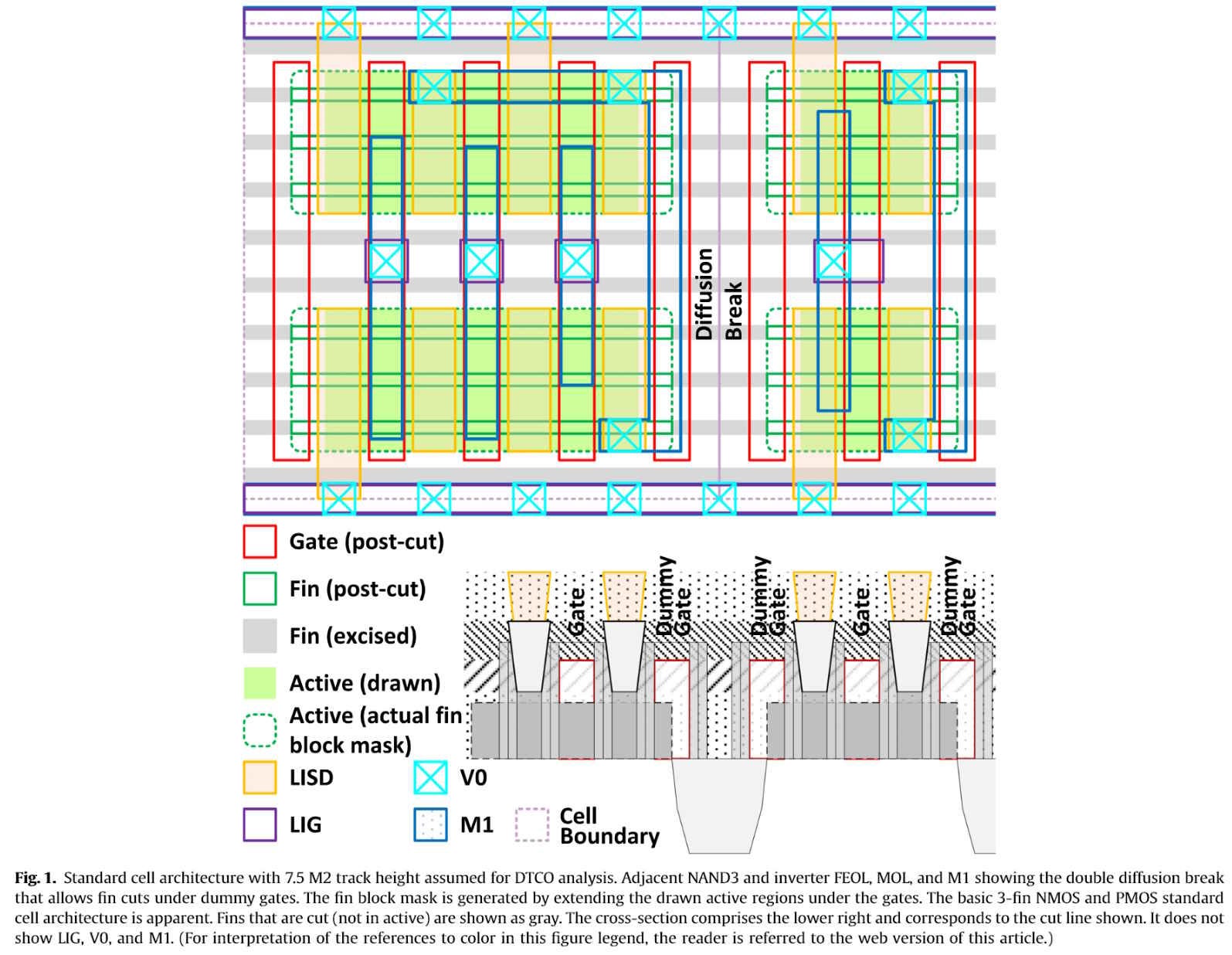
If you look at the Weste and Harris lectures online you will see they post some layouts for important logic cells. This raises the question, why am I not simply using those published layouts? The main reason is that the layouts are all for planar logic processes (their book and lectures are mostly dated around 2012, before FinFET was widely used) and I need FinFET. The CMOS transistors in the planar processes work much the same as they do in FinFET process, which means that the theory can be assumed valid if we do not get too complex, but the shapes and spacing rules are different so the cell layout will be quite different and this affects how they will all fit together, even if the electrical circuit used is the same form.
3D is very helpful to understand the cells. VLSI is not flat. Many standard cells are taller than they are wide. Intel 4 provides up to 16 layers of wiring above the FinFETs. The library cells I develop here will need at most 4 layers of metal, but that is enough to be thoroughly confusing with the traditional 2D multicolor picture (based on rubylith, again we find EDA conventions from the 1980s).
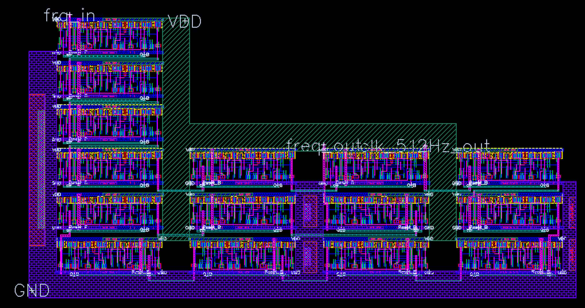
from A Digital Clock, by Yandong Zhang
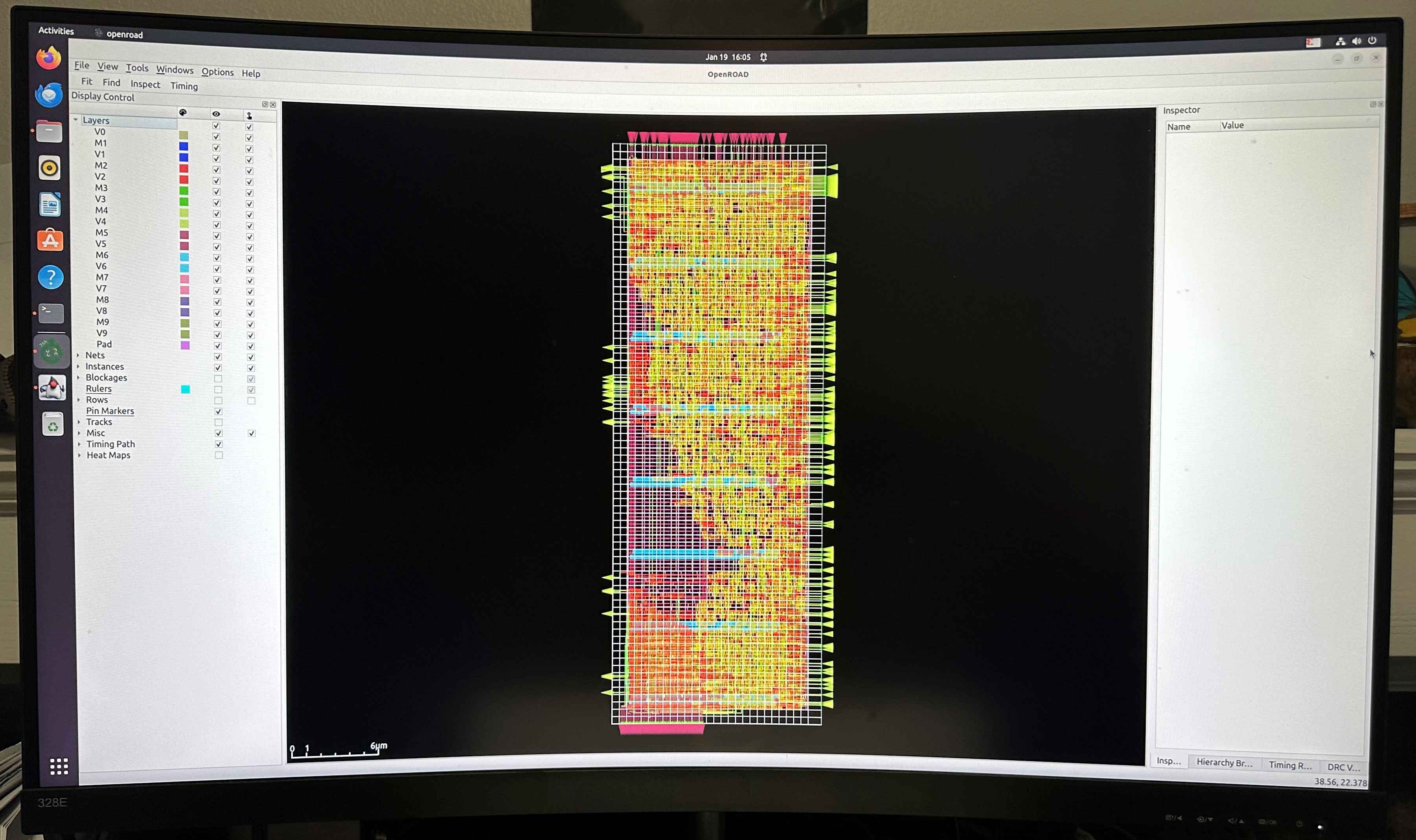
When using interactive EDA tools the flat view is pretty, but to make good use of it requires tedious cycling through with just subsets of the layers enabled, and you need good color vision. With a 3D image we can better understand the connections inside and between standard cells.
The 3D views are more instructive, so that is what I will use in this blog. Substack does not yet support embedding 3D objects into blogs (all browsers support WebGL 3D, so maybe someday). Instead, I will provide a mix of short videos and multiple static images to help see the structures from different angles and build up that 3D view.
The Cell Library is Central to EDA
The next post in the series will provide an overview of the imaginary library.