

Pipe 5: Clock pulses and adders
Pipe 5: Clock pulses and adders
Finishing up the basic library

NegEdge(CLK) Pulse Generation
If you have worked in Verilog you will have used positive or negative clock edge as a timing condition for your clocked logic. You might wonder how it works. Some circuits, like the D FlipFlop, only accept new inputs when the enable is positive, so the first thought might be to use flip-flops tied to the clock. The problem with that is that the FlipFlop would remain open to change for half the cycle, and in practice some things finish early while some things finish late, which becomes difficult.
In order to simplify this it is desirable for latches to sample values only very briefly, during the transition, and make that sample faster than any of the logic in a stage so that changed values arrive only after the sampling is done.
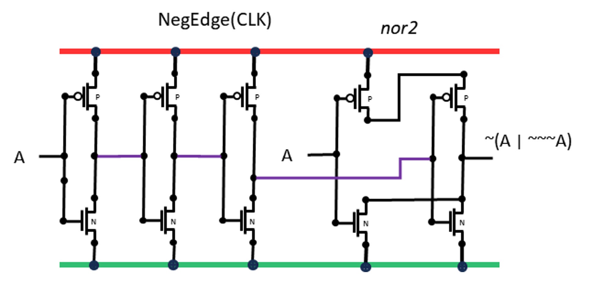
These circuits use the internal delay of multiple inversions inside a buffer cell to create a brief interval after a 1-to-0 edge when a NOR gate output will go true, then the delay closes and the NOR again has at lease 1 input true so the output reverts to 0.
The 3D models include a 3-inverter pulse width and a 5-inverter width. Analog simulation will help decide the width actually needed.
This circuit has a heavy use of energy as every transistor changes state twice on every clock cycle, while most of the SH-256 logic changes an average of 50%. The output will be buffered since each edge pulse will be driving the dynamic latches for typically 32 bits of latches.
In other ways the clocking requirements for the BlockChain SHA-256 pipes is quite permissive. There is no need for all stages to be synchronized, we just need close and reliable alignment between neighbors. Significant drift can add up along all 128 stages but there is no synchronous feedback from the end of the pipeline to the start. This loose constraint allows a systolic flow down the pipeline with slower clock drivers that consume less power. We will see more of this when the full SHA-256 digest pipeline is laid out.
More cell designs continue below the divider for paid subscriptions. Each week will have part of the blog open to all, then details then below a divider. The open part will help you judge if the work is of value to you, and I will try to keep it interesting by itself.
Thank you for supporting this work!
Variations on a Full Adder
We need a lot of full adders in the SHA-256, about 10 per bit (6 for the digest, 4 for the scheduler). Only 3 of those might need a carry look-ahead function where speed is justified even with the additional energy cost. We will look at how carry look-ahead works after working on a single bit slice of the full adder.
The basic functionality of a full adder has 3 inputs - A, B, and C (carry in) - and two outputs - S (sum) and Cout (carry out). The logic for a naive FA32 (3 in, 2 out) is
S = XOR3 ( A, B, C) = XOR2 ( XOR2 (A, B), C)
Cout = Majority3 (A, B, C)

There are some problems with this naive approach, mostly the input load. Each of A and B present 4 loads, while C presents 3, and the S output is weak. So there are some hidden buffers needed to make this work. I have not built a 3D model of this because it is clearly not the best.
A better solution inverts the inputs on arrival, reducing A, B, and C to single loads.

If you look in detail, you will see that every logic function uses negated inputs. The first XOR is replaced by an XNOR so that its output is negated to match the ~C used in the second XOR. Both the S and Cout outputs are now weak but generally the S output is going to drive a single output in another adder, except in adders using carry look-ahead which may need additional buffering. The Cout is not really changed since driving one inverter in the cell is similar to driving one inverter in the next cell.
This version can be implemented reasonably compactly. The single-track version has the most complex use of metal 1 and metal 2 yet, indeed metal 2 uses 4 out of 5 available lines which means other signals needing connection along the direction of the track will need to begin on metal 4.
Watch out for the Power Rails
In the videos for the single rail versions you will notice that the power rails on M2 are added in, along with some vias beneath them. Power distribution is vital and they take 20% of the M2 capacity, at least the way I use them here. M2 power rails parallel the M0 power to lower resistance and improve distribution. Droop in power is one of the main barriers to using low voltage and low voltage has a quadratic influence on energy, so I have been enthusiastic about distribution. In practice there will also be some cross-ties on M1 and M3 but at the moment it looks like capacity in those layers is not seriously constrained, with plenty of opportunity for cross ties to be added, so I have not made things more complex. But power rails seem to be a fixed constraint that cannot be added after the logical wiring.
Dual Track Layout
The smaller cells we have tried fit well into a single track - the space between one Vss and one Vdd, the lower and higher voltage power lines. However, the full adder is complex enough to wonder what happens if we spread across two tracks.
A two-track version is much easier to lay out with metal 0 and metal 1, no uses of metal 2. This would be more practical for the SHA-256 stage since there are multiple signals which need to bypass the adders along the direction for input to output. A 2-track design for the SHA-256 bit-level pipe is the most likely choice.
The Most Compact Design
Although this buffered circuit has much to like, with its light input load and good drive with likely good timing, it is not as compact as a widely used design developed in the 1980s and cited in several sources as a real-world CMOS choice.

This design also includes inverters but still requires 2 input loads for A and C, with 3 input loads on B. The main reason to like it is that it is more compact and has fewer transistor pairs, which gives it less energy need per operation, though it may be slower than the fully buffered version if it follows a cell with a weak output.
The single track version blocks all 5 of the M2 lines when the M2 power rail is added into the picture.
It may be possible in the 2-track versions to get a flatter wiring if the process allows gates to be continuous between the tracks. For example in the fully buffered circuit it would be possible to have 3 gates in the middle of the design, for ~A, ~B, and ~C, to simply flow together under the Vss metal and eliminate 3 of the M1 uses. There are similar opportunities in the minimal-size design which could elimnate one of the M2 uses. However, I stick with some conservative rules here to be more likely to stay comparable to real world design limits. If the real world allows some extra tricks then it just means things can be even better than the limits I will estimate.
The video shows 2 layouts, one with Vdd in the center, one with Vss in the center. These are not simple reflections, due to differences in the wiring solution.
The dual track minimal-size version blocks 2 out of 10 available M2 lines, a little more than the fully buffered version. That illustrates how a more compact design may also be more crowded to wire.
Next Week
The next post will introduce the logic of the Secure Hashing Algorithm SHA-256 standard and how this can be reduced to a small logical unit for transforming 8 bits, which will then be combined into larger groups eventually to obtain the full 256-bit width of hashing and 64 stages of that.