


Pipe 10: Doing the numbers
Back of the envelope estimates

This wraps up the series on the Digest pipeline for SHA-256. The design will be used to estimate numbers for size, energy, and speed.
The second half of this post will look at ways to optimize the pipes for even lower energy per operation.
There will be a one week pause before a series of posts begins on a new very-small topic in April.
Where does the energy go?
Energy goes into filling and draining capacitors when switching signals pass through. The largest capacitors are the gates of the transistors, which have various capacitance paths that can be lumped into a single number Ceff (effective capacitance) which summarizes the capacitance of a gate. It may be surprising that those small gates are such a big load, but their dielectrics are designed to be very thin and they need total control over the electrons in the transistor channel so they are doomed to be good capacitors.
The various layers of wires also have capacitance. The capacitance tends to be the same per unit length for small wires and large wires. This is because the capacitance is related to surface area divided by distance squared between surfaces Both scale together as the larger wires have larger spacing. A large wire high up the stack and it looks like that would be a huge load on a tiny transistor, like an ant carrying an elephant, but in practice that big wire has low capacitance for its size so it is if that elephant was a balloon. Process designers may succeed in making some layers better than others, but we will simplify our model with a single number Cw for the capacitance per micron of wire.
We use these numbers, Ceff and Cw, together with the supply voltage Vdd which is also the signal change in CMOS, in our calculations of energy. These numbers characterize a CMOS process just as importantly as the track height and transistor width do - but they are mostly not published. We will use estimates of 100 aF (atto-Farads) for Ceff, and 200 aF for Cw, which seem reasonable numbers found by searching the literature. A Vdd of 0.36 V is supported by the Intel paper on building the Bonanza Mine chip using Intel 4, which operated correctly down to 0.355V.

The size estimate is about 18,200 µm^2 for the 128 stages of Digests. With the Scheduler roughly 75% the size of the Digest, and overheads for data input and testing for success at the output, we can expect 30 pipelines per mm^2 (about 33,000 µm^2 per pipe).
Adding up the gates
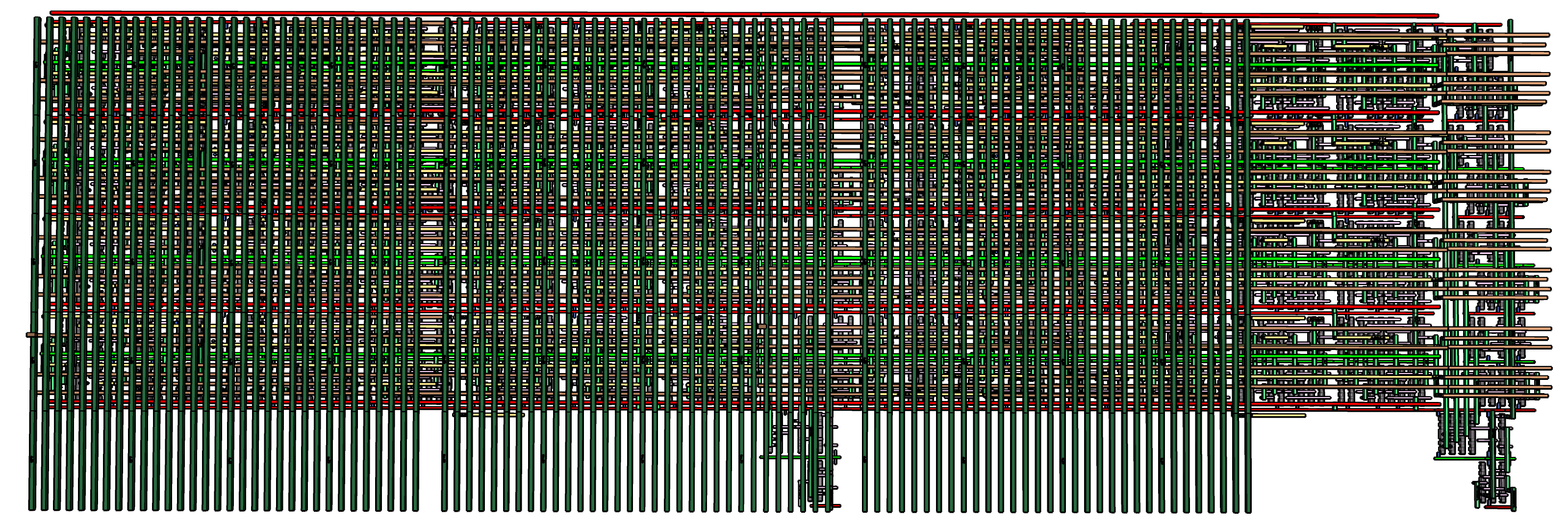
Here is a view of a 4-slice bundle drawing just the gates.
We can count the gates directly.

The gates which are used for clocking the input latches are counted differently from the other gates, because the clock gates cycle twice for every clock, while the other gates cycle only when logic values change.
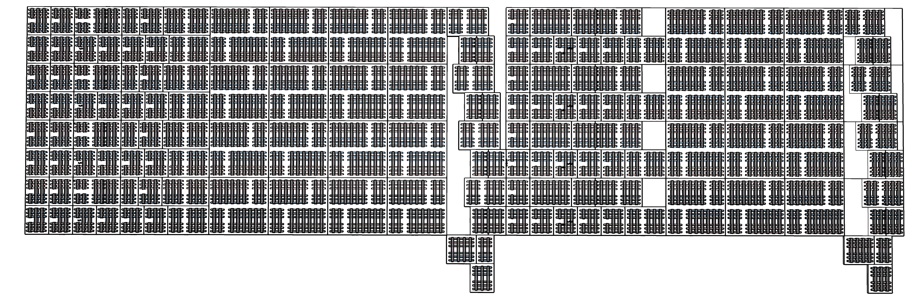
How long is a piece of metal?
A micron of wire is roughly the same load as a pair of CMOS gates. Each will be reckoned as 200aF.
M0 is the first of the metal layers.
M0 is used mostly inside logic cells.

We can estimate the percent coverage of the pattern to figure a value for the length of metal.
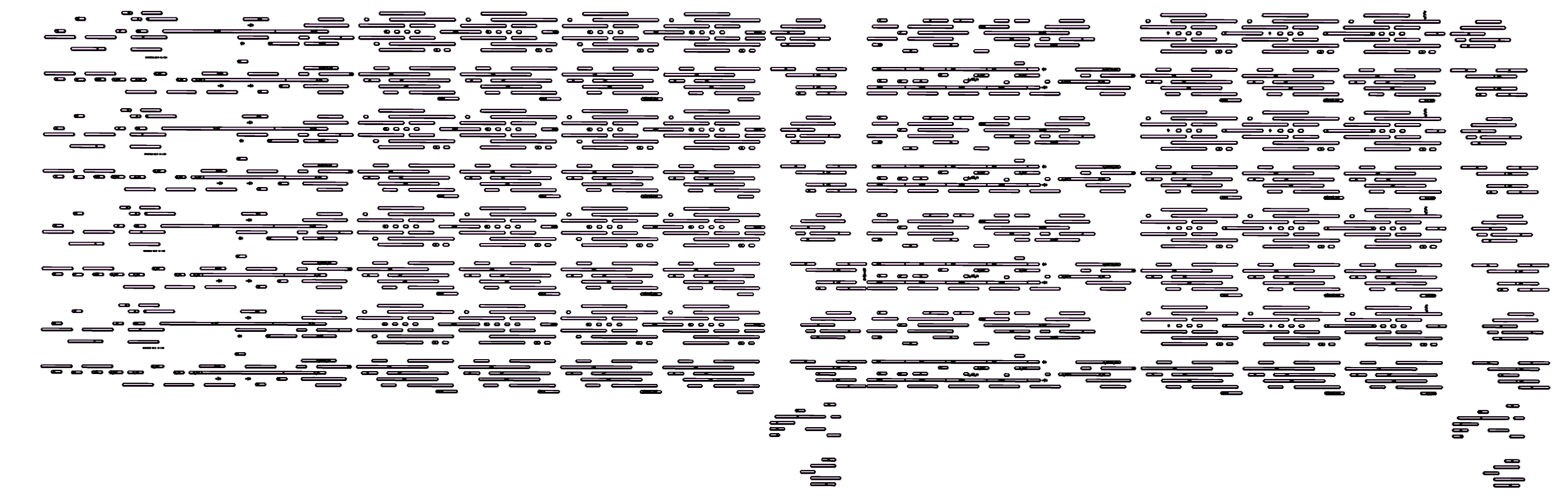
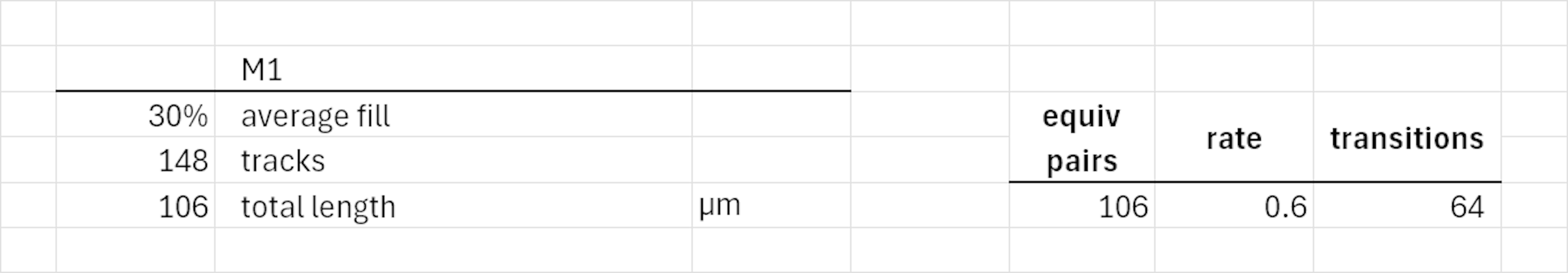
M1 runs perpendicular to the rail
It is used quite often, also mostly inside cells.

Many of these connections are short.
There are also a few longer runs to neighboring slices.
M2 runs the same direction as the rail

It is used a lot for connections between cells.
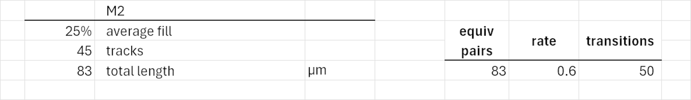
The percentage is kept low since there are no metal tracks counted for the median.
M3 is another sideways connecting layer
M3 is not used much in this design.
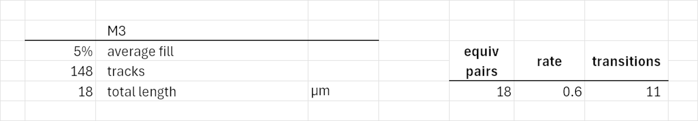
We could use it for rotation metals, since we have plenty of unused M3 tracks, but the M5 layer offers lower resistance for better long distance timing.
Metal 4 runs along the rails
It is a larger metal than those below.

M4 is used in this design mostly for longer connections which are inputs or outputs to an e- or a-pipe. The slice design is long and narrow, increasing the congestion on the M0 and M2 layers so there is still significant use for M4.
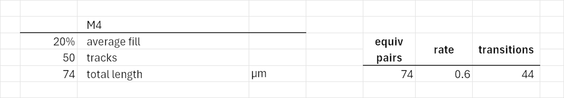
It makes a moderate contribution to the overall load.
Metal 5 is a larger metal running sideways
It comes in 3 sets. The actual lengths will vary when they span wide enough to reach all contacts, and they may be scrambled in order to reduce capacitative coupling. These might even split so some run in Metal 7 to increase separation and lower capacitance.

Although the image looks like a high percent the actual utilization is reduced if you look across all slices since the KW wires average half way, and the rotations will average about 80% length. The wires can end at their last useful contact.

M5 is used for the e- and a-rotation wires and for the kw input wires. It is preferred over the M3 layer because of the lower resistance makes a faster signal on these longer signal routes, some of which run over 20 microns.
Drum roll, please…
We are finally ready to estimate the energy, adding up the transition units from the gates and wires. Each stage contributes 1 clock of work for each hash, and there are 8 quad-slice groups in a stage with 128 stages in a dual-hash mining calculation, which is 1024 quad-slice groups in all to make one mining calculation.

This estimate is quite encouraging. We left out the clock drivers in the median, but they only need to drive 8 loads per quad-slice and they are easily synchronized laterally, so there are perhaps 30 to 40 transition units there. The Scheduler adds another 650 pair transition equivalents per quad for another 9 pJ/hash, and both the pipe input and zeros detection are kept simple, then the whole hash estimate should be around 25 pJ, which would be competitive as about the 3rd best in the market - and we have not discussed optimizations yet.
We will continue below the break with a discussion of possible optimizations.
I welcome discussion of the open section of the post, you can add comments to the Table of Contents for Pipeline post if SubStack will not allow your comments here. Thanks!
Thank you for supporting this blog.
Reducing fins and improved gates
The wire loads are just 2/3rds of the gate load, and the design has very few cells which drive a large load, so the whole design is probably a reasonable candidate for using a 2 fin per gate design. A quick and cheap way to do that would be to reduce fins from

to this — which might even be easier to make —

while leaving the rest of the design the same so that wiring is not more crowded. Switching to 2 fins has the potential to eliminate 15% of the energy needed.
Using weak pass gates for latches
20% of energy is going into the latches and the clocks that drive them. We can use an old trick to halve this - just use one side of the CMOS pair. Either the P or the N channel acts as a conductive path all by itself, the latch will operate if the other side is missing. It will just be a bit slower - but that added delay is just one iota of time in parallel on the 15 latches, none of them add up in sequence. FinFETs are well balanced in behavior of P versus N, so you can choose either. One of them may be slightly better.

It is important to choose the same kind for all the latches - either all have a weak pass gate with N, or with P. It is important so that we only need one polarity of driver and can eliminate half the drivers as well as half the gates. Another 10% saved!
Less Glitching
You may have noticed I assigned a 60% rate of change on logic, not 50% which seems more natural in a pseudo-random calculation. The reason is that values can glitch when inputs arrive at different times causing the output values (and internal states) of a cell to be indecisive, so that it changes momentarily and then changes back when another input arises.
An example occurs in the final full adders for the e- and a-pipe calculation. The pipes are designed to propogate most values in similar paths, starting with all inputs held on latches which release new values on the same clock edge, so most inputs arrive around the same time. But when we get to that final section there is a ripple carry within each group of 4. The lookahead structure limits glitching on the full adders to just the local 4 (and of those there is no carry input to the first so carry glitch effects increase to 50%, 75%, and 88% on the second, third, and final full adders. These have about 50% chance of passing on to the half adders. Thos have an additional roughly 55%, 28%, 14%, and 7% chance of another glitch happening when the forwarded carry arrives. These drive the rotation wires and their buffers, where there is a total of roughly 2 glitch transactions propagated to the a- or e- rotations per quad-slice group, or an overall average of one output glitch per slice. Each glitch drives typically a 16 micron wire with 3 loads, so that adds up to 20 extra transition unit loads per slice, or 80 per quad-slice, which is around 7% of the total transitions. Hence the general 10% “tax” added to logical transitions.
Can glitching be reduced? There can be some subtle improvements by choosing which input to use on which path to equalize path lengths. Most of the logic cells used in the SHA-256 have logically equivalent inputs but may have different loads and internal speed. For example all three inputs to a full adder are logically the same, but A and B have different input loading, and C has the fastest path to output. An EDA tool can help to analyze a balanced path.
What about latching, for example could we change the output buffer to an output latch before driving the rotation wires? The idea would be to time the latch until after the glitching, so that the glitch is not amplified into the large load of the rotation wires. Well, the latches themselves add some overhead. Weak latches would add 1 load unit per clock, and we could expect about 2 unit loads needed for the clock driver for the 4 outputs in a quad-slice. We will also need some cost for the delay circuit in the clock chain, in the median, which has to ensure that the delay between the output enable and the input latch on the next stage is long enough for the signal to propagate through the rotation wires. Let’s estimate that as a 4-stage buffer of some form, which (like all clock logic) transitions twice per clock. So, we add something like 15 unit loads to arrange these extra latches - but the payoff is saving an average of 80 unit transitions due to rotations glitching. That seems a good tradeoff. EDA tools can simulate the glitching and the solution.
With all of these changes - 2 fins, weak latches, and glitch reduction - we might be comfortably under 20pF for a full hash operation.
Better Transistors and Wires
Now we enter the realm of asking for miracles - but the process engineers keep improving things, right? Can we get a lower Ceff and Cw value from the process?
The fabs are very secretive about these parameters. Academic sources for my 100aF guestimate are a little out of date - maybe these numbers were right for 12nm, perhaps 7nm. Hopefully they have improvements. They might relax the gate control a little bit to allow a little more transistor leakage. Our transistors are switching 50% of the time so leakage around 0.1% should be ok, even though for other projects it would be awful. Low energy per operation is NOT the same as low power. The bitcoin mining chip is actually a hot, high power chip.
A more relaxed gate would in principle allow a reduced Ceff.
As for wires, we could ask for some reduced coupling between wires. Perhaps use of low-k insulating layers, and taller separations between layers. That would impact the impedance of vias which is a negative on speed, but does not necessarily mean higher energy per operation.
Should it run cooler?
Cooler junction temperatures mean steeper sub-threshold slopes so that transistors work well at lower voltages. If we can plan on seriously good cooling, like liquid immersion which does not itself take a lot of energy, then we can ask for the transistors to be tuned to run well at the lower target temps. A traditional server chip running at the power intensity of a bitminer would run about 30C hotter than we can arrange for an immersed bitminer, and that allows use of around 10% lower voltage if the gate work functions are tuned to match. If you want the cooling to work without using extra power it will also need to be sited in a cool climate or with plentiful natural access to water.
That is good physics, but not a normal ask of a foundry. Hard to say if such process tuning is available. It could be worth 15% or so in power, since that scales as V^2.
Will it be slower?
I’ll say it again: low energy per operation is not the same as low power. Not at all - indeed most of the functions like blockchain mining or AI inferencing where energy per operation will be important are definitely high-power chips.
For example, with 3,000 pipelines per cm^2 and 20 pJ/Hash, at a 1 GHz clock the chip will dissipate 60W per cm^2. That is supercomputer territory, similar to an Nvidia H100 GPU. A 1GHz clock is probably not difficult for the pipeline, even with some of the “slowing” added like weak pass latches and glitch suppression. The critical path is a 32-bit adder preceded by about 5 sequential simple gates in an 8-bit slice.
The limit to clock rate is heat. Improving energy per operation might make the clock rate faster, even it the technique used on the face of it seems to add delay. At the gate level the delay might be a few tens of picoseconds - enough time for signals to propagate along a rotation wire - while the clock cycle is stuck at 1,000 picoseconds due to heat. We need different intuitions about functions which have reached heat-limited density and clock. We need the EDA tools to help us navigate these tradeoffs.
How low energy can we go with new processes? I don’t know. But evidence is that Ceff and Cw are not changing nearly as rapidly as cell sizes, so for these energy limited functions we may already be near the limit. Maybe another halving of energy per transition can be expected - but it seems that even CFETs will not do that.
Next Week
Next week I will be taking a break, preparing for a new topic in April.
Did you like the Pipe series? Let me know in comments or in a message. Thanks!